|1.MP3 PLAYER|
2.7805 5V DC POWER|
3.MP3 PLAYER|
4.7805|
5.MP3 IC|
6.ON OFF SWITCH-2PLATE
7.TOUCH SWITCH ONE TRS|
8.CD 4017 TOUCH SWITCH|
9.TOUCH-I SWITCH ONE PLATE|
10.CD 4017 IR REMOTE CONTROL SWITCH.|
11|
12|
13|
14|
15|
16|
RESISTANCE-CONDENSAR.COLOR|
18|
19|
20|
21|
22|
23|
24|
25.RESISTANCE COLOR CODE|
26|
27|
28|
29|
30|
60|
|
| @1 1.AUDIO EMBED 2.AUDIO EMBED 3.WEB TOOLS 4.MULTI MEDIA 2.AUDIO EMBED |
| TW1
BUILD-ELECTRONIC-CIRCUIT
|
TW2
CIRCUITSCHEMATIC
|
TW3
AARONCAKE
|
TW4
HACKWEEK
|
TW5
EASYCIRCUIT123 | TW6 CIRCUITEASY | TW7 TALKINGELECTRONICS | TW8 IN.PINTEREST | TW9 CJFCUITFINDER | TW10 HOBBYTRONICS | TW11 DAILYMOTION | TW12 HOBBYTRONICS | TW13 HOBBYTRONICS | TW14 HOBBYTRONICS BOOK1 BOOK1 BOOK1 |
| - | - |
| C001. Remote Operated Home Appliances... Here is the circuit diagram of Remote Operated Home Appliances or Remote controlled Home appliances. Connect this circuit to any of your home appliances (lamp, fan, radio, etc) to make the appliance turn on/off from a TV, VCD, VCR, Air Conditioner or DVD remote control. The circuit can be activated from up to 10 meters. It is very easy to build and can be assembled on a veroboard or a general-purpose PCB. Parts R1 = 220K R2 = 330R R3 = 1K R4 = 330R R5 = 47R C1 = 100uF-16V C2 = 100nF-63V C3 = 470uF-16V D1 = 1N4007 D2 = Red LED D3 = Green LED Q1 = BC558 Q2 = BC548 IR = TSOP1738 IC1 = CD4017 RL1 = Relay 5V DC The 38kHz infrared rays generated by the remote control are received by IR receiver module TSOP1738 of the circuit. Pin 1 of TSOP1738 is connected to ground, pin 2 is connected to the power supply through R5 and the output is taken from pin 3. The output signal is amplified by Q1. The amplified signal is fed to clock pin 14 of decade counter IC CD4017 (IC1). Pin 8 of IC1 is grounded, pin 16 is connected to vcc and pin 3 is connected to D2 (Red LED), which glows to indicate that the appliance is ‘off.’ The output of IC1 is taken from its pin 2. D3 connected to pin 2 is used to indicate the ‘on’ state of the appliance. Q2 connected to pin 2 of IC1 drives relay RL1. D1 acts as a freewheeling diode. The appliance to be controlled is connected between the pole of the relay and neutral terminal of mains. It gets connected to live terminal of AC mains via normally opened (N/O) contact when the relay energizes. If you want to operate a DC 12 volt relay then use a regulated DC 12 volt power supply for DC 12 volt Relay and remember that the circuit voltage not be exceeded more than DC 5 volts. |
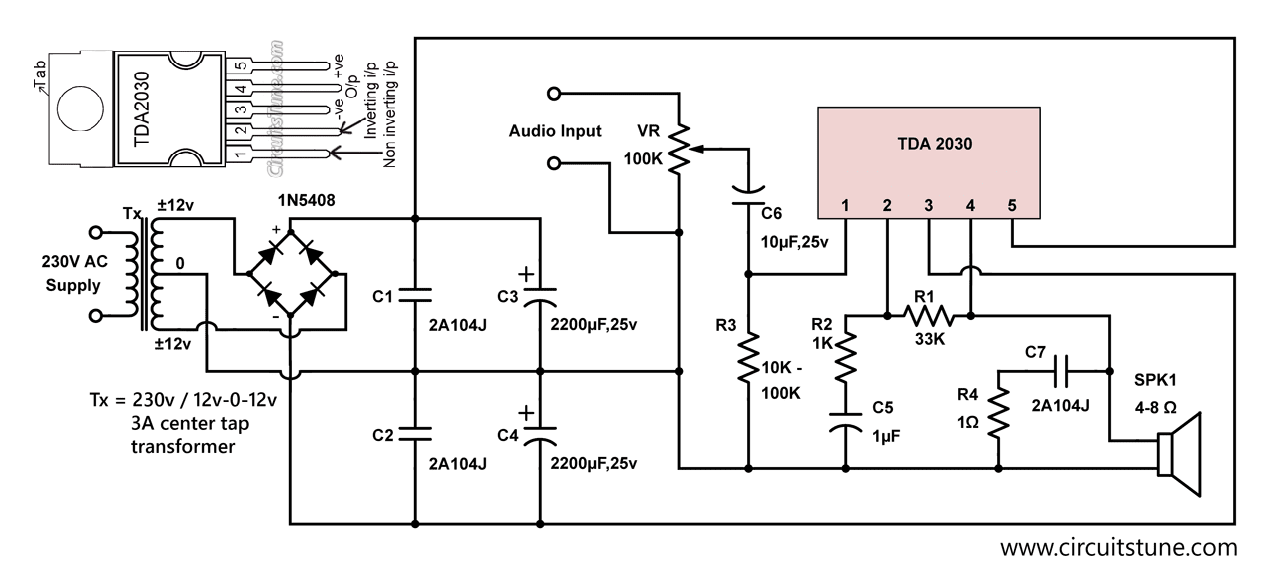
| C002 10W Audio Amplifier Circuit by TDA2030 The amplifier circuit by ic TDA2030 described here is an powerful audio amplifier with output power of 10W. TDA2030 is a monolithic IC, used as a low frequency class AB Amplifier. It has high output current and very low distortion. This 10W audio amplifier using TDA2030 is good for home/ small room. Circuit Diagram of '10W amplifier circuit using IC TDA2030' with power supply. tda2030 amplifier circuit Fig-1: Circuit Diagram of 10W audio amplifier TDA2030 Pin Diagram: TDA2030 Pinout Fig-2: TDA2030-Pinout/Pin-diagram Circuit Description: TX is a Center taped step down Transformer (230V,50Hz; 12-0-12,3A). For bridge rectifier use Diode 1N5408, 1N5407 etc. Use 10KΩ to 100KΩ as R3. VR 100K is a POT/Variable Resistor to control sound level. Capacitor C1,C2,C3,C4 is used as filter capacitor to reduce the ripple factor(AC element in DC). If ripple factor is high in supplied DC voltage of an amplifier, then output audio signal of that amplifier will be noisy. Remember that high ripple factor is responsible for high noise. The main attraction of an audio amplifier is its high output power and very low noise. For this requirement, this 10W audio amplifier circuit using this IC-TDA2030 is very good within low cost. Parts List Parts Value Name C1 2A104J CAPACITOR C2 2A104J CAPACITOR C3 2200µF,25v CAPACITOR C4 2200µF,25v CAPACITOR C7 2A104J CAPACITOR D1-D4 1N5408 DIODE R1 33K RESISTOR SPK1 4-8 Ω SPEAKER Tx 230v / 12v-0-12v 3A center tap transformer Transformer (Center Tap Secondary) U1 TDA 2030 IC Note: Use transformer with (12-0-12,3A) output voltage. Don’t use higher than 2200Hz,25V capacitor as C3,C4. That may damage the IC. Must use Heat Sink with the IC-TDA2030. Without proper Heat Sink the IC will be in risk of fry up Don’t use smaller than 1N54XX diode like 1N40XX, 1N40XX(ex:1N4001) may get damaged. We recommend to use four 1N5408 for bridge rectifier. All ground point in the circuit should be connected in a single point and ground it(If possible) or connect in transformers ''0'' marked wire as shown in the circuit. |
| C003 LA4440 Amplifier Circuit LA4440 is a dual channel audio amplifier IC. It can be used in two modes; one is Stereo amplifier and another Bridge amplifier mode. The LA4440 is a monolithic linear IC from Sanyo. Here I give the both circuit mode of amplifier using IC LA4440. Features of IC LA4440 It has 46dB of ripple rejection Low distortion Good channel separation Thermal protector Overvoltage protector Surge voltage protector LA4440 Stereo Amplifier Circuit When the IC LA4440 is Stereo mode in the circuit, its output power is 6w+6w. In stereo mode use two pieces speaker of 2Ωto8Ω. In the stereo amplifier configuration given below, C11 and C12 are output capacitor. But i ignore them from the circuit of bridge amplifier. Stereo Amplifier Circuit using IC LA4440 Fig-1: LA4440 Stereo Amplifier Circuit Diagram LA4440 Bridge Amplifier Circuit When the IC LA4440 is in Bridge mode in the circuit, its output power is 19w. In bridge mode use 4Ω-8Ω speaker. If you want stereo output(19w+19w) in bridge mode then use two copies of amplifier circuit of given below. Resistor R3&R4 is to adjust the voltage gain and for making input signal of inverting amplifier. Bridge Amplifier Circuit using IC LA4440 Fig-2: LA4440 Bridge Amplifier Circuit Diagram Circuit description for both, stereo and bridge amplifier mode C10 is filter capacitor used to reduce the ripple of supply voltage. Don’t decrease the value of capacitor C6&C7 less than 100uF, 10v, it may causes of the output at low frequencies goes lower. The pin-6 of LA4440 amplifier circuit is audio input pin; it used in stereo amplifier mode but in bridge mode it is grounded. C8&C9 are polyester film capacitor used to preventing oscillation, and R1&R2 used for the same reason as filter resistor. Though the maximum supply voltage for both circuit of amplifier is 18V but we recommend to use a 12V,3A power supply. Use a good quality heat sink with LA4440. I think here you see little comparison between stereo and bridge amplifier of LA4440. If you want to make this amplifier project, then I recommend you the bridge one. I think it is ideal for a beginner. And I love its wattage rather than Stereo mode. There is also a possibilities as I say, make two copies of circuit of bridge amplifier for stereo, it will give you 19w+19w of audio power output. |
|
COO4 M8031 ding dong circuit diagram This electronic circuit diagram is a ding-dong sound effect generator electronic device based on the M8031 circuit designed using CMOS technology. The circuit M8031 has a built-in RC oscillator and digital envelope circuits that make it to require few external components . The sound generated by the M8031 simulate an mechanical ding-dong sound. The M8031 operates from a low input voltage from 1.3 to 3.3 volts requiring low current . The integrated circuit is ideal for door bell application. |
| C006 USB Powered Audio Power Amplifier This circuit of multimedia speakers for PCs has single-chip-based design, low-voltage power supply, compatibility with USB power, easy heat-sinking, low cost, high flexibility and wide temperature tolerance. At the heart of the circuit is IC TDA2822M. This IC is, in fact, mono-lithic type in 8-lead mini DIP package. It is intended for use as a dual audio power amplifier in battery-powered sound players. Specifications of TDA2822M are low quiescent current, low crossover distortion, supply voltage down to 1.8 volts and minimum output power of around 450 mW/channel with 4-ohm loudspeaker at 5V DC supply input. An ideal power amplifier can be simply defined as a circuit that can deliver audio power into external loads without generating significant signal distortion and without consuming excessive quiescent current. This circuit is powered by 5V DC supply available from the USB port of the PC. When power switch S1 is flipped to ‘on’ position, 5V power supply is extended to the circuit and power-indicator red LED1 lights up instantly. Resistor R1 is a current surge limiter and capacitors C1 and C4 act as buffers. Working of the circuit is simple. Audio signals from the PC audio socket/headphone socket are fed to the amplifier circuit through components R2 and C2 (left channel), and R3 and C3 (right channel). Potmeter VR1 works as the volume controller for left (L) channel and potmeter VR2 works for right (R) channel. Pin 7 of TDA2822M receives the left-channel sound signals and pin 6 receives the right-channel signals through VR1 and VR2, respectively. Ampl i f ied signals for driving the left and right loudspeakers are available at pins 1 and 3 of IC1, respectively. Components R5 and C8, and R6 and C10 form the traditional zobel network. Assemble the circuit on a medium-size, general-purpose PCB and enclose in a suitable cabinet. It is advisable to use a socket for IC TDA2822M. The external connections should be made using suitably screened wires for better result. |
| RESISTANCE 10E# 15E# 18E# 22E# 47E# 68E# 100E# 170E# 220E-# 240E# 330E-# 470E-# ------ 1K# 1K5# 2K2# 3K3# 3K9# 4K7# 5K6# 6K8# 8K2# 9K1# 10K# 12K# 15K# 22K# 33K# 38K# 47K# ------ 56K# 68K# 82K# 100K# 120K# 150K# 220K# 260K# 330K# 410K# 470K# 5M1 |
| CONDENSAR 101=100pf=0.0001uf 102=100pf=0.001uf 103=10000pf=0.01uf 104=100000pf=0.1uf 105=1000000pf=1uf |
| -- |
| -- |
| -- |
| -- |


No comments:
Post a Comment